TRUE AGC AUDIO LIMITER
A dynamic range of 60dB without distorsion
To be used for RF transmissions or various volume compensation applications:
RETURN TO HOMEPAGE
Audio limiters and compressors are well present on homebrew oriented websites, and one could say that they might be classified into 3 types:
* First: Circuits featuring a few components (e.g a simple one transistor stage with a base bias circuit controled by a diode rectifier...) and stated to be audio limiters. In fact, except on a restricted dynamic range, they could be called audio signal clampers and distorders. I think that anyone having tried this kind of design will not be impressed by the performance...
* Second: Applications of professional audio IC's providing a very good performance (generaly designed for broadcasting or audio enhancement such as dbx or other equivalent principles). The schematics, directly picked from the manufacturer's application sheet, use components that are quite impossible to buy. In that case you'd have more chances finding a finished product on a broadcasting or free radio dedicated store website (great choice of compressors, stereo hi-fi encoders, and s.o...).
* Third: Designers of this last category circuits are generally well experienced and are proposing solutions with quite classical components, but the circuit is then very complex, using e.g ten operationnal amplifiers, multiple sophisticated feedback loops, accurate pre-emphasis, and s.o... For audio or broadcast fans it is an interesting adventure, but I think many people won't be courageous enough for a such work.
What I propose
I do not pretend proposing the ultimate audio product that gets out of the 3 categories by providing all the advantages. What I decided to design is a one channel (i.e mono) audio limiter (not a true audio compressor) being sufficiently easy to build and providing a correct sound on a wide dynamic range. The applications of that kind of circuit can be the following:
- Short range RF transmission, e.g. to get the sound of satellite radio stations on all FM radios in the house, without taking care on how the sat receiver volume is set. The circuit is then used beetween the audio source and a simple small RF transmitter (many available on the net). The same thing could be applied to any audio source
- Microphone preamplifier with AGC, compensating the great sound level variations that frequently occurs while using a microphone (the speaker distance to the mike and his voice strength vary a lot). This can be useful to insert it before an audio mixer (e.g. for comment insertion with the audio dubbing system for VTR presented on this site), before a low dynamic digital sampler (low cost voice recorder, toy...), or to build a sensitivity self adjusted intercom by putting a small audio buffer behind it.
- Advertising ''pump up suppresser'' by inserting the circuit beetween your TV audio output and your stereo audio amplifier. This will stabilize the average volume level, even if the volume is pumped up by the broadcaster during advertising (common practice in Europe and perhaps somewhere else).
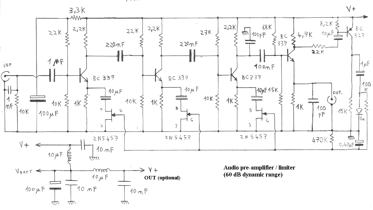
SCHEMATIC
Click on the schematic to see the enlarged version.
Circuit overview
The structure of this three stage amplifier is basic and looks like a school exercise about transistor amplifiers... Each emitter AC coupled resistor is replaced by a JFET (2N5457). One known property of this transistor is its behaviour for low voltage AC signals (less than 300mV, applied without DC voltage): Its current response is quite linear versus the drain-source voltage in both polarities, and depends on the gate-source voltage, so that it acts like a voltage controlled resistor. This will be useful to get a voltage controled gain for each stage. Since the goal is to get a good linear response on the whole dynamic range, each stage gain will vary only of a ratio 10, since the drain-source resistor is close to 100 ohms while the gate-source voltage is zero (maximum stage gain). Only the first stage features a low pass stabilizer on its base bias circuit. This will be sufficient if the power supply is actually delivered on the side pictured on the schematic (V+ and ground symbol), and if the ground connections are as equipotential as possible. (In fact you should apply the same board layout as the schematic drawing). If anyway you'd encounter unstability troubles (self oscillating), you could modify the base bias circuit of the second stage to get it like the first stage one.
Considering the rest of the circuit, the last stage is followed by a high pass filter-buffer (follower emitter) providing a lower output impedance. The output signal is compatible with a standard audio line input. The collector current of this buffer transistor causes a voltage drop on the 4.7K collector load. This voltage is used to ''trigg'' the PNP transistor (BC327) on signal alternances. As soon as it is trigged with a great occurence, the charge pump built around the ''Ge'' diode and the two capacitors (1uF and 0.47uF) makes the same negative voltage appear on each JFET gate, causing a gain decrease. Therefore the gain is self adjusted to get only a few peaks of output audio sigal above the PNP circuit trig level. The response time is shorter on gain decrease (negative charge of the 0.47uF capacitor) than on gain increase (discharge into its 470K parallel resistor), as it is always the case in that type of system. You might modify the values to get your prefered characteristics...
A last comment about the PI filters drawn on the lower left corner of the schematic: this is only useful for use with an RF transmitter (supplied by the ''optional V+'') . In any other case, only the ''Vbatt'' decoupling (100uF and 10nF) have to be used and ''Vbatt'' is directly connected to ''V+'' without inductor in series.
Setting up and checking
The circuit has to be used with a supply voltage of 8-13V. There is no particular set up to perform. As soon as you checked that the stages are correctly biased and stable, your audio limiter is ready to use. If you have no oscilloscope, the bias point voltages can be checked with a voltmeter and the stability simply by hearing the result...
Components alternative
If you don't succeed in finding the transistor references specified in the schematic, you'd have to take care of the following parameters for alternate components:
- BC337 and BC327: Icmax > 50mA, Hfe > 60, switching high speed transistors not recommended
- 2N5457: N channel JFET, Idmax > 10mA, gate threshold < 3V
- Diode ''Ge'': In fact, any signal diode, schottky (prefered) or silicium
Would you want to see other stuff like this ?
Return to HOME PAGE
Сайт создан в системе
uCoz