TIPS AND TRICKS - "HOWTO'S"
GROUND PLANES - THE KEY TO STABILITY AND RELIABILITY
If you have the possibility to make double layer printed circuit boards, this is the ideal situation. However in case of a first evaluation and taking into account the cost and the necessary tooling, you might prefer to use so-called "breadboards" for making circuits. Anyway, whatever you use a single layer PCB or a breadboard, for most of the proposed designs you will have to rely on a ground plane to obtain satisfying results. A bad ground equipotentiality can lead to more severe and unsolvable problems than a lot of people think, especially in analog circuits where high power and eventually RF parts share the same ground than small signal stages ! When talking about ground planes, I expressively mean a common ground connection plane where 0V nodes have to be
directly connected, and not just a plane connected at one point to the device ground. (This would be not only "less good" as a real ground plane, but this would be actually useless).
In all the present circuits exposed here you won't need separate grounds but one entire ground plane covering the whole component board area. The particular conditions where separate grounds are needed occur when high-end analog audio or high accuracy analog measurement chains must be totally protected against low frequency disturbances. (E.g. mains hum, switched mode power supplies) and when no significant current flows through the 1-point ground return path beetween the two planes (unless the two blocks are totally independent and no connection exists at all). I've added this remark to avoid starting any debate about the "good way to design ground pathes" according to various and opposite dogmas.
The most important thing is that noisy and sensitive parts do not share one same connection point (aka "via") to the ground plane. This practice also presents the advantage of eliminating the need of ground tracks on the circuit board. This allows to obtain easily a clean and homogeneous layout.
Here is a "pure homebrew" method for building an efficient and low cost double layer circuit (single sided breadboard + ground plane) which gives very good results, even for radio circuits up to 150MHz.
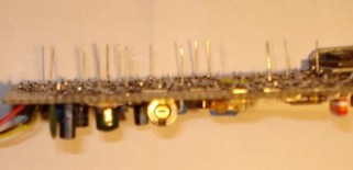
First, component pins to be connected to ground are left uncut when assembling the circuit...
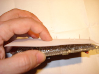
Then, a paper sheet is used to record easily the position of all ground pins...
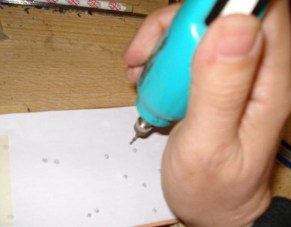
The paper is used as a grid for drilling holes into the copper ground plane...
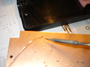
And finally, the ground plane is inserted and soldered.
To test basically the device before mounting the ground plane (DC bias points, power supplies...) it is still possible to connect temporarily ground pins together by using a wire.
Proceeding like this avoid having many unexplained functional troubles in the devices, unless you are a real expert able to avoid the numerous traps of common ground impedance by optimizing the circuit layout... ;-)
DECOUPLING CAPACITORS AND IC GROUND CONNECTIONS
Anybody says that ICs must have their power supplies equipped with decoupling capacitors, and anybody says that these capacitors must be close to the IC power supply pins. But what a lot of people like to forget is that it is as much important to have a short connection to the Vss (negative) pin as to the Vcc (positive) pin, even if it seems logical. When using a ground plane the problem is easily solved because it is just necessary to place the capacitor close to the Vdd pin and to connect Vss and the capacitor negative terminal both separately to the ground plane. (The ground plane presents a low resistance and a low inductance). When no ground plane exists, if a ground loop of several centimeters connect the capacitor to the actual Vss pin, consider that there is practically no decoupling capacitor here. ;-( Let's keep in mind that decoupling capacitors are aimed to source very short current peaks to the ICs when required and that these current peaks could cause a significant self-induction effect in a simple track inductance. Therefore no significant inductance must be present beetween the capacitor terminals and the IC power supply pins !
STAR WIRING OR NOT ?
This is also sometimes a big debate: Is it sometimes allowed not to implement star wiring on a PCB ? Many disputes have started and will start about this subject. But what we can say, if talking in the simplest possible way, is the following: When no signals are travelling from one stage or block to another, these blocks must of course be all connected to the power source without sharing the same common line impedance. This applies without exception. This is star wiring, even if it never looks like a star. ;-)
But things may not be so clear and simple if the different blocks or stages are exchanging signals, and particularly small signals. When not using a ground plane, a star wired ground would induce strong spurious AC voltages beetween the respective grounds of both stages, e.g. output stage of an amplifier and the previous stage. This occurs because each stages creates its own ground offset versus the power source ground. This could even lead to unstability. This is why sometimes a less usual way to proceed gives better results, when no real equipotentiality is possible: The noisiest stage is the first step of a ground chain wiring (starting from the power source) and the previous stage is the next step, provided that no other part shares the ground line from the output stage to the previous stage. The most important thing here is that there is no AC voltage present beetween the two stages grounds.
This small example can make you afraid when thinking about all which can occur on a complex circuit and about all the unclear tricks that you may have to apply... In fact in this case my goal is reached ! Now you know why I insist so much about the use of a ground plane. The real subject is finally not: "Star wiring or not ?" but: "Thanks to the ground plane I can always rely on star wiring and have no headache"...
Return to home page
Сайт создан в системе
uCoz