Contactless and batteryless remote sensors
Simple solutions and surprising results.
This is one example of many recent applications from effects discovered more than one century ago.
RETURN TO HOMEPAGE
The circuits proposed here are using no custom (i.e unfindable) IC but still be usable too with existing passive tags (called RFID tags) at low frequencies (e.g 125KHz).
Basic principle
As every student knows, conductor loops have the following properties:
- Generation of a magnetic field when a current circulates into the loop
- Induction of an AC voltage on an open loop when submitted to an alternating magnetic field
- Circulation of an AC current if the loop is closed
- Self induction leading to the presence of a series equivalent impedance (while used as reactive load or as induced electric generator): Z = pulsation x inductance.
This page is not intended to be an exhaustive information source about magnetism and coils (generally school and university websites have some interesting pages about this subject).
Its purpose is to expose the actually most used methods to get the maximum performance beetween:
- A field generator coil with tuning circuit allowing a maximum drive current for a limited driving voltage available.
- An induced coil (with tuning circuit too) providing a maximum voltage on a defined load (the sensor or ID tag)
This main requirements are leading to the following typical layout:
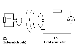
The better way to get a maximum current into the ''transmitting'' coil (since generated field is proportional to it) is to tune it in series while driving the LC tank with a voltage generator. As the tuned circuit resonnates so that the impedance is minimum at the resonance frequency, the design of the voltage source is simplified: there is no need to generate a true sine wave voltage, since harmonics of the source signal will cause a current witch can be neglected in respect to the fundamental, while the LC tank Q factor is high enough (the value 5 is my reference). This will result in a simple switching push-pull design and a low loss rate into the driver output stage, so that there will be no need to use heatsinks. Furthermore since in that way it is possible to source a quite high current into the coil while keeping a high inductance value, the coil can consist into many turns and have a wide area so that the generated magnetic field is much higher. The limitations of this tuning are:
- The Q factor and the bandwidth (totally linked): If the Q is too great, the bandwidth will be very narrow and any drift of one component (capacitor, driver frequency, coil shape alteration) will have drastical effects. As a reference, an absolute maximum Q about 40 is realistic if you are using standard components (especially for the capacitor). That's why often designers add a series resistor into the tuning circuit.
- The coil inherent series resistor and the capacitor ESR witch are limiting the possible current into the LC tank. Even if you are using low resistance wire to wrap many turns, the Q factor limitation requirement will force you to increase this series resistor, and this will result into a current decrease most significative than the increase of the field/current ratio.
Then the better way to achieve a maximum voltage induction (for a low sourced current) thanks to the ''receiving'' coil is the use of a parallel resonant circuit. Considering the global Q factor (parallel load included), this is a good way to maximise the voltage at a magnitude of Q times the coil unloaded induced voltage. But of course the same restriction applies for the Q factor value as for the transmitting coil. Like in this first exposed case, if you try compensating the Q, while increasing the inductor, by adding a series resistor, you will loose more than you'll gain, particularly if your RLC equivalent parallel impedance (L2.W2/R-series) exceeds the magnitude of the load equivalent resistance.
Now, one could say that this is good for remote powering of low consumption loads but that the coupling quality at a useful distance spacing will not allow us to send back any information to the transmitting coil (primary) by connecting and disconnecting the load or something like that, since the effect will be undetectable...
In fact, it is true if we are talking about a simple current sensing or about an absolute comparison of the field transmitting tank overvoltage amplitude (L-C middle node) to a fixed threshold. This way to proceed would offer a very poor reliability. That's why existing systems such as many RFID tags (most current application at this time) actually use load switching to send back some data, but this is done thanks to a coding witch generates regular signal periods, so that absolutely no DC signal is taking part of the information. The most commonly used schemes are the Manchester and bi-phase encodings. Their advantage is a signal average value witch is not depending on the data content, so that this modulating signal (very low modulation rate on the transmitter side) can be easily picked (at the L-C node), demodulated, filtered and amplified with usual simple techniques without major risk of deformation.
Of course, when you design your own system, some more simple information can be managed, such as: frequency of the switching (modulation) signal, presence or not of this signal, or cycling of modulation bursts (since duty cycle modulation of the switching signal itself is not recommended for the reasons exposed here above). The simple ideas exposed in this page will focus on such techniques and will allow you to design many types of contactless sensors.
DRIVER SCHEMATIC
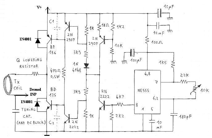
Circuit overview
No particular surprise in this circuit where I once again used a NE555. However, any square wave generator can by used. I have choosen this one because it is a simple way to get an adjustable frequency. This feature is helpfull (although the goal is to set it at 125KHz definitely) to do a fine tunning of the transmitting LC tank.
The half H-bridge gets an interesting power ability (coil current up to 1A) and should not require more than a small heatsink on each BD13X (witch can be a 6mm� piece of PCB with a full copper layer). C1 and C2 should normaly not be needed, except if output transistors (e.g. alternate components) are heating (causing an abnormal current consumption) even without any load connected (detailed further). The ''Demod inp'' connection point has to be connected to the demodulator input (see below). A particluar care must be taken for the board layout, especially for ground lines. It is seriously recommended to apply the following way to proceed: Build your board (e.g. ''veroboard'' with pads) without routing the ground lines, except for very short links beetween component ground terminals. For each equipotential point (where ground is therefore missing) obtained in that way, leave one component pin not cut. Then when you are finished, use a copper covered board (board for PCB's bought without sensitive resin) as ground plane that you will put 5-8 mm under your component board. Solder each uncut component pin to this plane, as well as the output and power supply grounds. This will be much easier if you drill the ground plane, so that you solder on the copper face opposite to the component board side.
DEMODULATOR SCHEMATIC
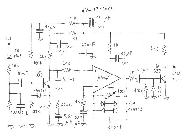
Circuit overview
This AM demodulator is intended to exctract first the signal enveloppe featuring a very weak modulation signal (classic diode demodulator on the left using ''Cd'' to be defined further), and to amplify this useful signal while rejecting the strong residual carrier noise. That's why the circuit features several low pass filters at each stage of the chain. The final (high gain) amplifier uses an OPA on witch a signal amplitude limiter has been added (feedback loop featuring 4 diodes) in order to avoid saturation witch would cause a bad behavior of the OPA. As the demodulated signal is square wave shaped, this non-linearity causes no problem at all. The gain can be adjusted, depending on the noise present when no sensor/tag is sending back the data. Finally, on the right, a simple switching transistor is used to get a logic level signal, usable by any digital circuit (frequency meter, retriggerable monostable, microcontroller...). Note that the same layout recommendations as for the driver are relevant here. The supply ground of the demodulator must be taken from the driver ground plane (where the main power supply ground is connected), or better, it will share this same ground plane.
SENSOR INDUCTION INTERFACE EXAMPLES
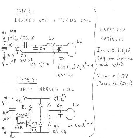
Notes about this two kinds of tuned induced circuits:
- The RL resistor in type 2 has the following role: To keep a sufficiently high supply voltage while DATA is active. It has to be chosen versus the LC tank equivalent parallel resistor (sensor equivalent load in parallel
with Lx2W2/RLx). Then the RL calculation is only a question of voltage divider. The fact you need it or not depends of the duration of the DATA-ON periods versus the current consumption of your sensor, considering the 4.7uF capacitor.
- For type 1 the RL resistor is not necessary while the mosfet RDSon is not too low. Else the same RL calculation than for type 2 applies, except that only the Li coil impedance (Li.W) has to be taken into consideration here (quite a low impedance).
The main design recommendations are:
- Lx >> Li (applies for type 1). Li should probably be imposed by the environment and will have to be measured (e.g. with a signal generator, by seeking for the cut-off frequency of a L-R network...). Then, Lx = 20 x Li appears as being a good choice. Note that if Li is already higher than 100uH, the type 1 method looses interest.
- Lx values must be compatible with a tuning capacitor in the range 150pF-10nF.
- The equivalent load to the sensor electronics (Rload) should be equal to W2.(Lx+Li) / Rlx, with Rlx = Coil Lx series resistor. This will allow a maximum energy transfer. Then the same Q factor requirements apply, as in the reader study (see further about bandwidth). The global Q will be: (Lx + Li).W / (2 x Rlx) if the optimal energy transfer condition is fulfilled.
- To assess that the sensor electronics will be powered with a sufficient voltage, this global Q plays a major role : Vsupply = Q x Li_Unloaded_Voltage. This defines the Q lower limit.
- For type 1, the Li coil series resistor has to be as low as possible (maximum modulation effect possible).
- The type 1 and type 2 modulation circuits will have opposite effects: While setting DATA=1, the type 2 induced coil current decreases (resonance killer) while the type 1 induced coil current increases (load resistance decreasing).
Here are some sensor electronics given as examples:
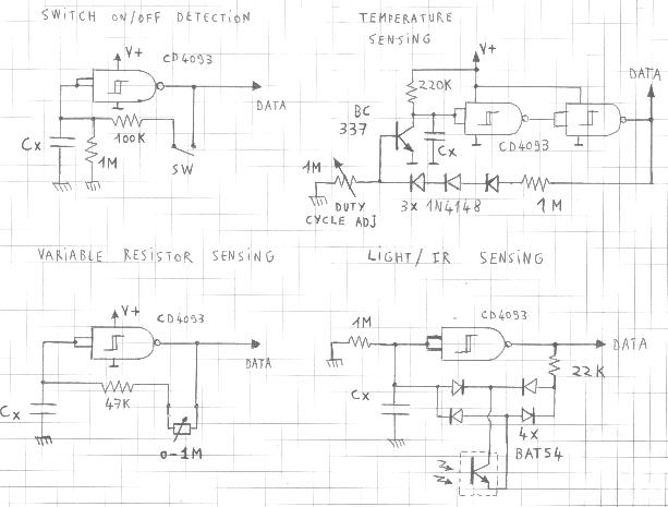
General overview
This sensors do not pretend being industrial accurate measure tools. However then can be useful for many applications requiring a poor accuracy (e.g 10%) or boolean data (detection/no detection), as well as more accuracy demanding applications where the distance from the ''reader'' transmitter and the temperature are stable, considering that the returned data is managed as non-linear and to be corrected. Furthermore it is always possible to adapt sophisticated low power sensor IC's in such designs and to get robust systems, quite insensitive to temperature and distance (influence of the distance is due to the influence of the supply voltage in the sensor when using trics like those exposed here). Even the use of a microcontroller sending back encoded data (e.g. PIC16LC84) is possible, while extracting the CPU clock from the received carrier (I let you put your creativity in action for that, now you have the keys to design remote batteryless sensors...). Note that the Cx value in the examples (to be expected in the range 1nF to 22nF) has to be adjusted into real operating conditions to get the required data frequency (I prefer telling you that instead giving values that you would probably have to modify). The recommended range that I'd give you is 1.5KHz to 7KHz (4KHz typical).
Comments about the two main kinds of LC tank
The circuit using one induced coil and one tuning coil that I propose is less efficient in terms of induced voltage, but has the following advantages:
- Simplified modulation switch circuit
- Use of standard components possible for the tuning coils
- Low inductance possible for the induced coil, giving the possibility to build or use one turn loops, while their area is wide enough. (This is useful in the case where you use an existing structure as a loop and place the sensor on it...
- No risk of ''zero modulation effect'' in case of approximate tuning of the sensor (this can happen in the other circuit type when the de-tuning occurs so that the phase shift in the LC tank is 45 degrees).
That's why I suggest the use of this type of circuit for homebrew designs, although the other one is the most used for integrated applications (RFID sticks, dedicated IC's) because of the small volume and the lower cost.
Setting up and checking
An oscilloscope is absolutely necessary to set up this circuits. A signal generator would be welcome. The power supply (driver and demodulator) can be within the range 9-16V, but shall be perfectly stabilized and filtered. Any medium frequency residual waveform amplitude as low as a 1mV could make the sensor data demodulation quite impossible.
WARNING
This type of device is able to generate high currents into a resonant circuit, resulting into high voltages on the ''Demod INP'' potential (more than 200V possible). As the current can reach 1A, the use of coil tuning capacitors rated for this use (e.g. polyester or polypropylene capacitors specified for this AC current or for a corresponding AC voltage at 100KHz) is seriously recommended. That's why I shall not be hold as responsible in case of capacitor explosion or electric shock leading to any material dammage or personnal injury. As you are warned you have to decide if you are experienced enough to proceed at your own risk by applying the content of this web page.
- - -
Tuning the reader-transmitter and its LC-tank, design of the LC tank
I propose the following procedure for the LC tank design (everyone might have his own one):
- How much current can source your power supply ? This will directly give you the maximum current ''Isupply'' that you are allowed to use. When the LC tank will be perfectly tuned, the half H-bridge output stage will sink an average current equal to Isupply for a peak current into the transmitting coil of pi x Isupply (the current is sourced by the power supply during the half of the period, and within this half period the average current is 2 x Ipeak/pi). This requirement then directly gives you the impedance of the LC tank at resonance, i.e the total series resistance (coil wire + eventual resistor). For that do not forget to apply the ratio 4/pi on the driver voltage amplitude since it is the fundamental amplitude coefficient. Note that your interest is to use the maximum allowed current since for a same Q factor, a low current cannot be compensated by turn number increase (inductance increases faster than the field).
- What is the required Q factor ? Two restrictions apply on it : the possible tuning drift (limiting the Q factor at a maximum of 40 as explained above) and the maximum frequency ''Fmod'' of the modulation signal from the sensor (witch must not be damped by the LC tank response). This consideration is valid on the sensor side too. My reference for a 125KHz carrier is Q < 125 / (2 x Fmod), with Fmod expressed in KHz. (This is deduced from empirical tests witch can be justified by AM modulation spectrum considerations where a square wave shaped signal must at least get its fundamental signal unaffected and its third harmonic not too attenuated).
- Then the inductance can just be deduced as: L = Q x R / (2 x pi x 125,000). Since the shape of your coil is probably imposed by your mechanical environment, you just have to define the number of turns required to get the calculated value. I suggest to choose the inductance value closest to the calculation allowing the tuning with a standard capacitor value (from the classic law LCW2 = 1). To estimate how much turns you have to wrap (do 10% more than the estimation to be able to correct), you can use this calculation tool from E.J. Edwards (amateur radio ID: G4FGQ) witch covers a great field of cases.
- Then there is no more secret to be revelated for the capacitor choice, since we just have defined it in the same time than the inductor.
- The last parameter to be defined is the actual series resistor. The calculation tool probably returns a too high Q factor with the wire that you planned to use (else you are lucky) and a lower series resistance than the one defined (same thing said in another way...). That's why you will have to add an actual resistor in series with your LC tank (I do recommend to insert it on the driver output side) to get the required total resistance value.
Your LC tank is now designed, then you have to tune it experimentally. For this, proceed simply this way:
- Put the driver on, first unloaded, with the frequency set at the minimum (adjustable resistor at its maximum value) and check that its output signal and its current consumption are normal (square wave signal, low current i.e < 100mA DC). Then adjust the driver frequency at 125KHz.
- Connect the LC tank and put the oscilloscope probe on the series resistor terminal opposite to the driver output (i.e LC tank side). In case of a perfectly tuned circuit, you must see the following type of signal:
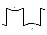
This is an evidence of a zero phase beetween current and voltage. Note that the incurved form has to be symetrical for that.
- If the signal is not the one expected, change the driver frequency until getting the correct waveform. Then calculate the actual inductance value (thanks to LCW2=1) according to the frequency that you had to set. You can correct the resonance frequency by adding a capacitor in parallel to the existing one if the actual resonance frequency is too high (normally it won't happen since you took care of the 10% margin for the coil turns), or decrease the number of turns on the coil if the actual resonance frequency is too low. Of course you can decide to keep the LC tank as it is and to operate at its frequency (not equal to 125KHz) but anyway you will further have to tune the sensor LC tank according to this frequency. Note that when not operating at 125KHz, you loose the compatibility with a lot of RFID tags and serial solutions existing on the market.
Particular note about the driver itself
If you notice some abnormal heating of the output transistors and a current consomption higher than 100mA even when no load is connected, add the C1 and C2 capacitors (enhancing the anti-overlap feature beetween the complementary transistor controls) by trying several tests starting from 1nF. As soon as the problem is solved, do not set more capacitance than required (else you might induce another heating cause by increasing the switching times).
Tuning of the sensor LC tank
Whatever is the sensor selected type, it has to be tested complete, with the electronics connected to the LC tank (real load conditions). If a signal generator is available, I suggest the following method (the most operator friendly...).
- Do not power your sensor in the ''normal'' way (i.e with the reader magnetic field) but inject a signal into the ''receiving'' (i.e induced) coil via a 470 ohm series resistor (10K for type 2) and thanks to the signal generator (sine waveform, frequency preset at the driver frequency, e.g. 125KHz). Put the oscilloscope probe so that you can view the voltage signal on the tuning tank output.
- Make the generator frequency deviate from its nominal value to check how much the tuning has to be corrected (same remarks as for the reader LC tank). Proceed until the amplitude is maximum for the required operating frequency. Of course you'll have to set the generator signal amplitude so that the sensor clamping zener does not play its role.
If you have no signal generator, simply use the reader with its coil untuned (capacitor equal to 10 times the required one) to be resonance insensitive on the reader side. Note that in this case you will have to get the sensor very close to the transmitting coil since its performances are drastically altered. After that, the way to proceed is the same as with the generator. Here you will use the driver frequency adjust feature to check the sensor tank resonance...
Checking the demodulator, adjusting Cd and the gain
Before starting directly the checking of data demodulation from the sensor, just put the power supply of the demodulator on, without injecting any signal at the input (reader LC tank disconnected or driver off). Check that the bias points are normal (transistor not saturated and OPA output at this transistor collector voltage) and that the circuit is stable (no noise nor oscillations) whatever is the position of the gain setting adjustable resistor. Then set the gain at the minimum (resistor at zero).
You will have now to define the value of Cd and place it. To do that easily, first turn the driver on with its LC tank connected without connecting the demodulator input. Measure the actual overvoltage at this point (set your oscilloscope and the higher V/div scale) witch might be slightly different from the planned one, then apply the following formula witch guarantees that the residual carrier signal amplitude will be less than 0.5Vpk-pk (Targetting a better rejection could affect the useful enveloppe demodulation):
Cd = 8.10E-6 / ( 10E5 x ln[VP/(VP-0.5)] ), where:
- Cd is expressed in Farads
- VP is the measured peak voltage
- The 8.10E-6 coefficient apply for a 125KHz frequency (period expressed in seconds).
It has to be changed for other frequencies.
(This formula is simply deduced from the classical RC discharge law within a time period equal to the carrier period.)
Of course, after calculation take the closest standard value available, since this capacitance is not a critical parameter. Note that Cd has to be DC rated at the peak voltage (e.g. 200V if it is the case).
Then after you mounted Cd and put the complete system on (driver, LC tank and demodulator connected), operate it first without any sensor and start turning the gain setting trimmer until the noise level is just high enough to attack the output transistor (logic level translator). Then go back so that:
- No more pulses are viewable on this output, for applications with on/off sensor types.
- A few sharp pulses are viewable on this output, for applications where the sensor is always sending back modulation (allowing more sensitivity).
Then you just have to get your sensor closer, and see if the results are compliant to your expectations...
Possible applications, and expectations that you could have
This list of possible applications is no exhaustive at all, but I just wanted to show you how many they can be, by imaginating for example:
- Rotating part with embedded sensor (e.g wheel carrying a wide loop as Li)
- Sensor located into a liquidproof compartment, to be readen from the outside
- Access control (door, PC keyboard activation,...) where the ''sensor'' is a user carried badge (even for pets).
- Data transmission accross an obstacle witch cannot be cut / drilled. This ELF fields can cross concrete and even thin metal planes.
- Contactless switches in a complex mechanical environment
- Part position checking (''sensor'' always on detectable when facing the reader)
If you have other ideas, don't hesitate to mail me (contact on home page).
What could you approximately expect from the systems described here ? Some of my experimental results can help you to estimate if your wishes can come true: (tests done with a simple unstable 4093 gate as data generator).
Example 1:
- Transmitting coil of 60cm2, 60 turns
- Transmitter current at 1A peak
- Sensor: one loop circular Li coil with a 15cm radius (circuit type 1)
-> Reading distance about 30 cm.
Example 2:
- Circular transmitting coil with a 3 cm radius, 40 turns
- Transmitter current at 300mA peak
- Sensor: one loop circular Li coil with a 3cm radius (circuit type 1)
-> Reading distance about 8 cm.
Example 3:
- Circular transmitting coil with a 3 cm radius, 40 turns
- Transmitter current at 200mA peak
- Sensor: small ferrite rod as Lx (circuit type 2)
-> Reading distance about 5 cm.
Note that this indications are for guidance only and shoud not be taken as accurate data.
Anyway I am ready to receive new ideas and photos of your applications...
WARNING
As you may have heard or readen, the current status of knowledge about biological effects of ELF fields has led to several official guidelines, such as the ICNIRP document dealing of occupational and temporary exposure to electromagnetic radiations (from ELF to microwaves). For information about the subject, you could visit for example the website of EMF Links. Considering this fact, I do not encourage you to use huge transmitting loops (e.g. around doors or windows, surrounding a whole room, etc...) driven with high currents (things you could be tempted about to get high performances) in order to avoid high rate occupational exposures. As you are warned about this particular issue, I shall not be hold as responsible for any effect and/or consequences (proven or not) of the use of ELF transmitting systems.
- - -
Components alternative
If you don't succeed in finding the transistor or OPA references specified in the schematic, you'd have to take care of the following parameters for alternate components:
- BD135 and BD136: Icmax > 2A, Hfe > 80, Ft > 50MHz, de-saturation time < 100ns
- 2N2222 and 2N2907: Icmax > 50mA, Hfe > 80, Ft > 100MHz, switching transistors
(de-saturation lower than 100ns)
- uA741: Output impedance < 1K, Slew rate > 2V/us, Gain-bandwidth > 1MHz, garbage < 2V respective to Vdd and Vss, compatible with 9V single supply operation or 4.5V symetrical supply operation.
- BC337: Icmax > 50mA, Hfe > 80
- 1N4001: Any rectifier diode rated for at least 2A, recovery time < 100ns
- 1N4148: Any silicon signal diode
- 2N7000: Small signal N-channel mosfet, Rdson < 10 ohms with Gate voltage = 3V, Coss < 150pF.
- Polarised capacitors: Any electrolytic or non-polarised type is OK. No voltage higher than the power supply exists beyond the demodulator blocking capacitor, nor into the driver circuit.
- BAT54: Any signal schottky diode rated for at least 10mA.
Would you want to see other stuff like this ?
Return to HOME PAGE
Сайт создан в системе
uCoz