Simple DC-DC down converter without dedicated IC
A simple and reliable switchmode regulator with high efficiency
The only IC used in that design is one of the most well known IC's in the homebrew amateur world.
RETURN TO HOMEPAGE
Voltage converters causing a minimum of power losses (opposite from linear regulators) are sometimes necessary when the voltage ratio beetween input and output is high, and where at least one of the following requirements applies:
- Battery operated appliance
- Small volume converter with no thermal dissipation possible
- Power source current rating lower than the required supply current of the low voltage rated load.
Possible application examples are:
- Car battery adaptater for 3-6V appliances, such as portable player or stereo, pocket TV, handheld video game appliance...
- Used battery ''energy sucker'': Place 3 old sets of too discharged batteries (that you kept) into an external battery compartment connected to (or taking part of) your converter. Then supply your appliance (using normaly 1 of this battery set) with the converter at its normal supply voltage. Since the voltage conversion is done with a low loss rate, the current sourced by the batteries will be 2-3 times lower than for direct use. Therefore it will be possible to ''suck'' the rest of the energy available in the batteries (discharged battery series impedance increases generally more than unloaded voltage decreases). Don't do that with rechargeable batteries, else you will seriously affect their lifetime.
- Applications where a quite high voltage (e.g. 12V) at low power and a low voltage (e.g 3V-5V) at a higher power are needed. Using the converter from 12V to 3-5V allows the use of a single 12V battery pack for both supplies with a correct lifetime.
- Power losses reducer if used before an accurate linear voltage regulator (e.g for 5V digital circuits...) not suited for high power dissipation.
Basic principle
Whatever is the switchmode converter regulation principle, at least one inductor (or transformer) is present, providing an interesting way to get this two main effects:
- Current averaging while applying a switched voltage
- High voltage burst generation by applying a switched current
These are the key of all low loss voltage and current converter principles.
The circuit exposed here uses a simple self-regulation method witch do not need careful stability considerations. As the drawback of this method is a small residual AC signal surimposed to the DC output voltage, a simple active filter (causing less than a 10% loss rate for a 6V output) is added. (It might be suppressed for non electronic power demanding loads). Furthermore this power supply will be able to withstand temporary overloads (inrush current from the load).
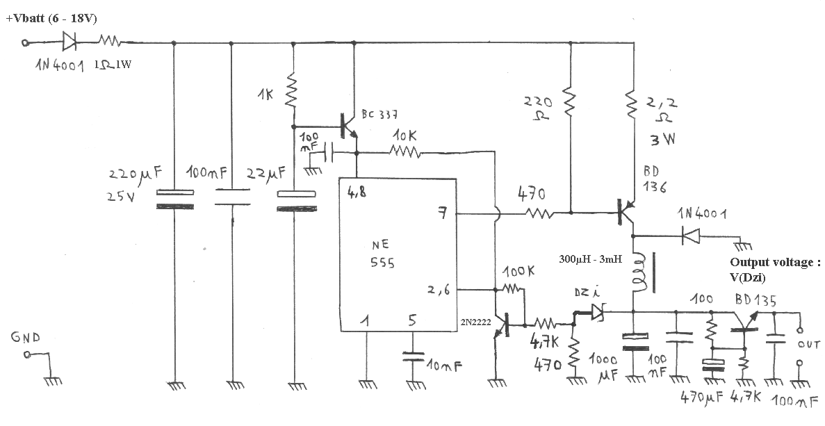
SCHEMATIC
Click on the schematic to see the enlarged version.
Circuit overview
Once again, I used the well known NE555. Here its purpose is to act as a low hysteresis trigger (input on pin 2-6 via 2N2222 transistor) witch will drive the coil switching transistor (BD136 via open collector output on pin 7). The only purpose of the BC337 transistor is to filter the power supply voltage of the IC (in case of high impedance of the power source). The system simply operates as follows: As long as the charge level of the output 1000uF reservoir capacitor (charged via the inductor) is to low, the zener diode ''Dzi'' is not biased, so that the NE555 stays with its output in the active state (BD136 activated). In case of a time limited surge, the current limitation provided by the 2.2 ohm emitter resistor makes this current switching transistor be able to withstand this temporary stress. Then when the 1000uF capacitor charge level reaches the required level, the zener diode and the 2N2222 transistor make the IC toggle to an inactive state of the pin 7 output (open). As the global hysteresis of the system is low, as soon as the charge level has decreased of some 200mV, the switching transistor is turned on again, and this cycle perpatuates. Whatever is the power consumption at the output, the duty cycle and frequency of the switching control will be the result of this controlled instability, so that the output voltage will always be equal to the ''Dzi'' zener voltage (switchmode converter generates Vdzi + 0.6V and the follower emitter active filter substracts 0.6V). Of course the 1N4001 diode purpose is to ensure that the coil gives its energy back on switch-off (without producing voltage peaks witch are a loss cause and a danger for the switching transistor). The coil value is not critical as well as it is compatible with a sufficiently low frequency (switching limitation of the components) and it has a low DC resistance (recommended: no more than 1 ohm for one ampere of output current, 10 ohms for 100mA, ...). Very big coils are useless and could make the system loose its advantages (weight and volume), but you can use a quite small used transformer secondary for that purpose (while leaving the primary open - do not touch it in operation !) as well as its DC resistance is low enough.
Setting up and checking
The circuit has to be used with a supply voltage of 6-18V and the ''Dzi'' zener voltage can be selected within the range 3V3 to 12V. (Out of this range, the converter efficiency over 12V and the voltage accuracy below 3V3 have no more great interest). There is no particular set up to perform, but try first with a test load (power resistor or lamp) to check that the converter works properly. As soon as you checked that all is ok, your converter is ready to use. This circuit shall not be care sensitive, but it is recommended to keep the positive supply voltage and ground distribution lines as short as possible beetween the set of decoupling capacitors (on the left) and the power switching circuits (on the right) to get a clean output voltage. The 100nF decoupling capacitor for the NE555 has to be shortly linked to pin 8, and its ground terminal shortly linked to pin 1. The same recommendation applies for the 10nF capacitor on pin 5.
Maximum ratings:
Although I did not check that, the maximum output current rating assessment is 1A permanent, sourced by the output for a 12V input voltage. The device withstands at least a 1 second long short-circuit (self limited at 1.3A, switching transistor de-saturated). Longer short circuit withstanding will depend on the presence of a heatsink on the switching transistor (BD136). Anyway, for loads sinking more than 500mA, at least a small heatsink is recommended for this transistor. Furthermore in that case the 100 ohm resistor of the output follower emitter transistor should be lowered to 33 ohms.
Boosting the gear
If you really want to use this design for high current power conversions, i.e for more than 1 ampere sinked on output, the following modifications can be done:
- Replacing the BD136 (switching) by a high power transistor (lower Hfe because darlington components have a very long de-saturation time).
- Driving this switching transistor by inserting a follower emitter PNP to build a ''discrete darlington'' structure: collector to switching transistor collector, base to existing divider, emitter to switching transistor base with 470 ohm pull-up to positive supply. This is faster than a classical darlington circuit.
- Changing the existing 470 / 220 divider to: 470 / 330
- Decreasing the emitter resistor of the switching transistor to the following value: 2/Io ohms (with Io maximum output current in amperes).
- Replacing the BD135 by a high current NPN darlington transistor, and compensating the additional 0.6V drop caused by this: insertion of a signal diode in series with the base (anode to base, it is not an error) and pull-up resistor added from this base to the positive supply (e.g: 820 ohms for a darlington Hfe equal to 10,000).
- Increasing the filter 470uF capacitor up to 1000uF.
- Lowering the zener diode bias resistor from 470 ohms to 100 ohms.
This modifications are not recommended for low power operation since in that way they cause useless power losses.
Components alternative
If you don't succeed in finding the transistor references specified in the schematic, you'd have to take care of the following parameters for alternate components:
- BD136: Icmax > 3A, Hfe > 80, Ft > 10MHz, de-saturation time < 0.5us
- BD135: Icmax > 3A, Hfe > 80
- BC337: Icmax > 100mA, Hfe > 80
Would you want to see other stuff like this ?
Return to HOME PAGE
Сайт создан в системе
uCoz