Smart capacitive sensor using no custom nor rare IC
It uses only 3 OPAs and some discretes.
This circuit is of great interest in case of integration of the capacitive sensor into a complete system managed by microcontroller. Its purpose is to convert the imaginary part of the impedance present on the detection plate into an analog DC voltage.
RETURN TO HOMEPAGE
Several principles of capacitive sensors do exist. The one used here is an accurate measurement of an AC admittance.
Basic principle
As the goal is to be conductance insensitive, the way to proceed is the following:
- Application of a sine wave voltage signal to the detector plate
- Voltage conversion of the current sourced to the detector plate
- Sampling of the converted signal at the source voltage zero crossing point
- As the current can be decomposed into a zero phase part (due to conductance) and a 90 degree part (due to capacitance), the current capture at the voltage zero crossing is only sensitive to the capacitance.
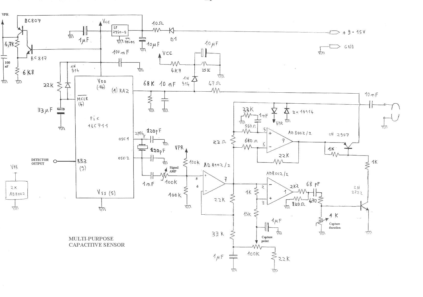
SCHEMATIC
Click on the schematic to see the enlarged version.
Circuit overview
The PIC711 microcontroller is the one I used for my application, but any microcontroller with built-in A/D converter would be convenient, as well as the clock generator is based on a quartz or ceramic resonnator in the range 1-3MHz. Of course, for a stand-alone smart capacitor application, this circuit looses its major interests, since it becomes in this case quite expensive and complex, compare to a dedicated IC (such as the quite recent Quantum smart capacitive sensors using charge transfer technology). This schematic is intented to be a part of a main board featuring the full system functionnalities, so that the components really used for the sensor are the 3 OPA's, 2 transistors and the passive components surrounding them.
- The sine wave signal taken from the uC resonnator output (clock driver input) is first buffered by a first OPA. The level can be adjusted thanks to the ''signal amp'' adjustable resistor.
- Then the buffered signal is injected to the detector plate via a 22 ohm series resistor. A differential amplifier (upper OPA) connected to this resistor enable us making a current to voltage converter.
- In the same time, the lower right OPA acts as a comparator, providing a square wave signal. The ''capture point'' setting is intented to get the square signal edge exactly corresponding to the voltage ''DC average crossing'' (since here only the signal AC part has to be taken into account).
- The RC derivator followed by the two transistor circuit is a simple way to make the capture without the use of a true sample and hold circuit. At each rising edge from the square signal, the 2N2907 PNP transistor is saturated within a short time, charging the 10nF capacitor (drawn close to the uC A/D input) at the sample level. No fast decrease of this capacitor charge is possible on quick negative variations from a capture to another (only discharge by its parallel 68K resistor), but this is not an issue since detected variations are in the field of human possible moves. The capture time window is adjusted thanks to the ''capture duration'' adjustable resistor.
Setting up and checking
An oscilloscope is absolutely necessary to set up this system. A double trace oscilloscope is recommended.
Start with ''Signal amp'' at the maximum resistor value, ''Capture duration'' at the zero resistance value, and ''capture point'' at the middle position. Note that the uC oscillator must be running, even if you did not make the programm yet. The detector plate terminal shall not be connected, even to a wire.
- First check that the AOP power supply voltage is about 7V to 8V.
- Then turn the ''signal amp'' trimmer to get a 4Vpk-pk buffered signal.
- Ensure that the output signal of the differential amplifier (upper OPA) is lower than 300mV pk-pk. Else minimize it by trying this two possibilities (one shall work): high value parallel resistor on the 33K to ground or on the 22K on feed-back.
- If a double trace oscilloscope is available, match the square wave signal edge to the bufferd signal ''DC average crossing'' by using the ''Capture point'' trimmer.
- If no double trace oscilloscope is available, place a 4K7 resistor beetween the detector plate terminal and the ground (current in phase with voltage), then look at the 2N2222 collector voltage, while turning the ''Capture duration'' trimmer until sharp negative pulses are surimposed to the sine wave. After that, set the ''Capture point'' trimmer so that the sharp pulses occur at the sine wave DC average crossing point. The 4K7 resistor can be disconnected.
- Then in any case, look at the 2N2222 transistor and set the ''capture duration'' trimmer so that the sharp pulses typical width is around one tenth of the voltage signal period.
- Connect the detector plate and look at the DC signal present on the uC A/D input. Variations of this voltage must easily be seen while approaching the detector plate. Note that the shape and the surface of the detector plate is a determinating parameter, as well as the presence of a ground plane or connection of the ground to a metallic structure (that improves sensitivity).
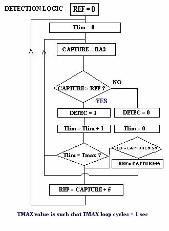
RECOMMENDED MANAGEMENT ALGORYTHM
As this circuit is intended to fit to many different microcontrollers, I just propose a diagramm showing the main steps of the information processing. This will allow the best performance:
- Self calibrating
- Reference self-correction on stable capacitance increase
- Immediate reference self-correction on capacitance decrease
This will avoid any permanent false detection and any sensitivity loss while the environmental conditions are changing.
''RA2'' is the uC A/D input converted value (corresponding to the schematic example) and the ''+5'' increment applies for a 8-bit converter (multiply by two for each additional bit).
Components alternative
If you don't succeed in finding the transistor or OPA references specified in the schematic, you'd have to take care of the following parameters for alternate components:
- 2N2222 and 2N2907: Icmax > 50mA, Hfe > 80, Ft > 100MHz, switching transistors
(de-saturation lower than 100ns)
- AD8002: Output impedance < 100 ohms, Slew rate > 200V/us, Gain-bandwidth > 50MHz, garbage < 1.5V respective to Vdd and Vss, compatible with 7V single supply operation or 3.5V symetrical supply operation.
- BC807 and BC817 (SMD components references): Icmax > 100mA, Hfe > 50
(e.g: BC337 for NPN and BC327 for PNP)
- LP2950-5: Any 5V regulator (choice depending on the rest of the board)
- 1N914: 1N4148 or any silicium signal diode
Would you want to see other stuff like this ?
Return to HOME PAGE
Сайт создан в системе
uCoz